
Spatially integrated electronic circuit carriers are connected using 3D-MID technology (MID: moulded interconnect devices), which allows for the direct coupling of mechanical, electrical, and optical functionalities on injection moulded components or films. The PCB tracks are directly incorporated into the casing and take the place of the usually printed circuit board in this application. The 3-dimensional component geometry of the MID-technology allows for a great degree of design freedom while also allowing for shrinking and weight reduction at the same time.
Fields of Application with Safety Implications
MID-technology is at the heart of several safety-relevant sectors of application, such as, the automobile industry. It is necessary to ensure that the MID components continue to perform properly in this environment, despite the challenging surroundings and preconditions. In addition, medical technology, communications technology, measurement technology, and analytical technology, as well as aircraft, are typical domains in which MID-technology is used to great effect.
Following are the processes that are used to manufacture MIDs, which are based on current state-of-the-art technology:
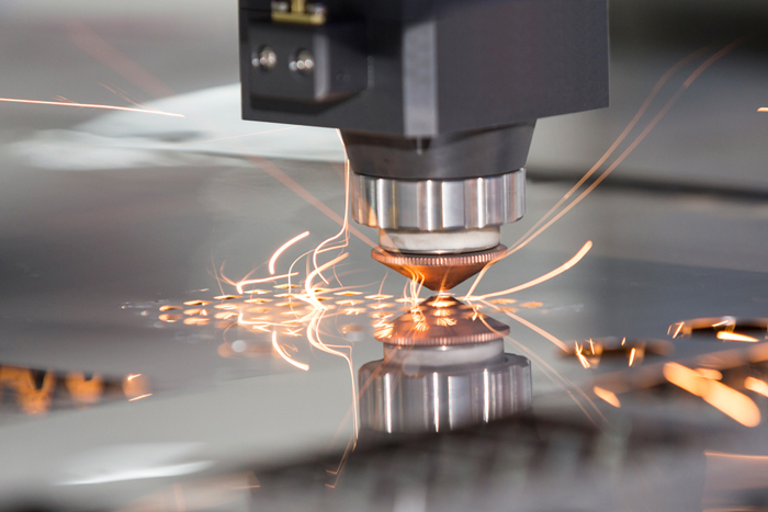
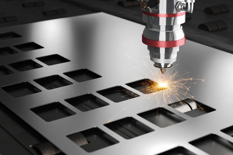
- Using a laser, direct shaping may be achieved (additive and subtractive)
- Injection moulding with two components
- embossing using heat
- Injection moulding with a film back
The metallized thermoplastic part (MID) is used to replace the mix of printed circuit boards and components, which is typically made up of a variety of different materials in most applications. The 3D-MIDs are composed of recyclable thermoplastics and can be disposed of more easily than traditional printed circuit boards.
Circuits can be produced more cost-effectively and quickly using MIDs, and design modifications can be performed and implemented in less time with MIDs than without them. Electronics using 3D-MID are now found across the whole spectrum of the industry. The 3D-MID is the right choice if a greater level of integration of the electronics is needed, such as when space and weight savings are required.
Metalization is a term used to describe the process of transforming raw materials into finished products.
The https://www.teprosa.de provides sample metallization, process assessment, and testing services for the full metallization process, from conception to completion. For large-scale metallization series, we collaborate with experienced partners that have a wealth of knowledge and expertise in metallization technology.
Technology
Copper, Nickel, and Gold Electroplating on Plastic Chemical Copper, Nickel, and Gold Electroplating on Plastic
Assembly and packing
When it is essential, we may package electronic components utilising the pick-and-place approach for modest numbers of electronic components. For bigger series, we collaborate with highly qualified partners that have a wealth of knowledge and expertise in the area of 3D-MID.
- Assembling/Picking and Placing
- Soldering in the Vapor Phase
- Bonding using Conductive Adhesive
- Aluminum Wire Bonding is a kind of bonding in which aluminium wires are bonded together.
- Process of Flipping the Chip
In addition to certification and validation of your component, our MID services are completed. Through the utilisation of our in-house test laboratory, we are able to get important insight into the product’s behaviour in real-world settings. These revelations are then included into the manufacturing process itself.
In addition to being well-established as a leading technology for the production of 3D antennas for mobile phones, the 3D-MID technology (three-dimensional moulded interconnect devices) is also gaining a strong foothold in a variety of other applications such as MEMS packaging, sensors, LEDs, switches, and connectors, and it has the potential to become a game-changing technology due to its abilities to miniaturise, rationalise, and integrate functionally. Miniaturization is enabled by the integration of mechanical and electrical functions into a single component, allowing for far more compact construction and a significantly higher function density to be attained.